
Home » Wafer Foundry
Category Archives: Wafer Foundry
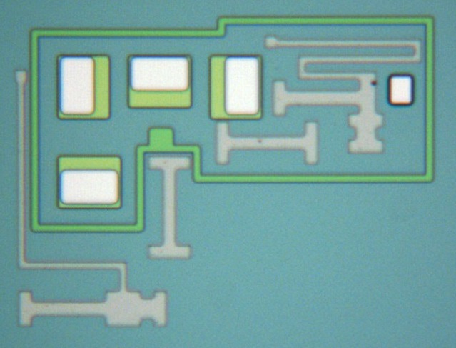
DAPike Engineering capabilities improved with addition of high power microscope
The addition of a high power microscope substantially adds to DAPike Engineering’s skillset. The high resolution system can measure critical dimensions down to 1 um. The following photos demonstrate the capability.


This allows us to document the dimensions of photo masks on the various layers of an Integrated Circuit or measure the sizes of defects found on silicon wafers. These high resolution photos can be very helpful when trouble shooting yield issues or setting up processes during process development.
Please contact us if you need this service.
Great visit to the Bay Area of CA in September 2016
An excellent trip took place in September during which multiple customers were contacted as potential foundry partners for Semefab, Ltd. I was joined by Allan James and Neil Wotherspoon and visited with the following potential MEMS foundry customers; Solid State Optronics, Posifa, Siargo, TSI Semiconductor, JVD Inc, Twist Semiconductor and Isobaud, Inc. Also a phone conference was held with Nevada Nano.
The products produced by the MEMS companies ranged from Mass Flow sensors to Molecular Spectrometers and Optoelectronic switches.
Another trip for Semefab is scheduled for January of 2017 to the Bay Area.
Customer visits in San Jose, CA
Last week, I visited with two clients, a silicon foundry and one potential customer during a busy business trip to San Jose, CA. The clients were Semefab, Ltd and AllWin21, for whom I am sales representatives. These successful companies; Semefab which has a growing business in wafer production with MEMS devices a key growth area and AllWin21, located in beautiful Morgan Hill, which has an excellent product line of Plasma and RTP wafer processing tools.
In addition, I visited the 4″ silicon foundry which I recently selected to produce my customer VerAvanti’s chip. The engineering manager and I inspected several of these MEMS wafers and confirmed the process is under control. Next on the schedule was Isolink a potential customer and the manager who is an old friend which could turn out to be a great source of future 6″ foundry wafers for Semefab. All in all, a great trip was enjoyed to the green hills of the Bay Area.
2015 Trip to Semefab in Scotland


An entertaining and educational trip was made in September 2015 to Glen Rothes, Scotland the headquarters of Semefab Ltd, a world class silicon foundry for which I am the North America Sales Manager.
A reunion with Allan James and John Bruce was just what was needed to reacquaint me with the upgraded capabilities of Semefab’s very clean wafer fabs, consisting of three separate facilities. There is ample capacity in 6″ to support the customers needs in any technology specifically CMOS, Bipolar, DMOS, and MEMS. Please contact me if you need any foundry services.
Allan and John treated us all to lunch at the Covenanter Hotel in Falkland where I enjoyed staying almost 20 years ago during my first trip to Semefab.
Custom Integrated Circuit nearing completion for VerAvanti
 The first silicon for the custom IC designed and fabbed for VerAvanti is in the final wafer processing stages. This has been a rewarding but challenging project as I had to design not only the IC chip layout, but also custom develop a silicon wafer process to fit the design and identify a suitable wafer foundry. This unique MEMS device will allow VerAvanti to fabricate a microscopic video camera used in Endoluminal imaging for patients requiring angioscopy.
MEMS wafer foundry visit to the Northeastern United States
An early November visit was made to the Northeastern US to present Semefab’s capabilities to several customers. Two companies were visited in the Boston area. One is a start up in the early stages of establishing their process and one is a founder of the MEMS technology. Needless to say that the start up was very receptive to our presentation while the bedrock company was much less so. I also was hosted by my brother in law, Eugene Sgrignuoli who supervises maintenance and gave a detailed tour of his plant at Vicor, the leader in small footprint modular power supplies.
I was fortunate to be entertained by friends and relatives the entire trip and had multiple meals of lobster, calamari, crab and mussels while consuming many varieties of the great craft beers of New England.
Next I traveled to the Eastern Pennsylvania/New Jersey area. Two customers and a university, Lehigh, my alma mater were visited. The first was a very promising business involving print head technology. It uses a non-silicon very large scale chip with a very good fit to Semefab’s process technologies. The second was less promising as it was a very small company already serviced by a 150 mm foundry. The last visit was to Lehigh University where I was hosted by my long time friend and fraternity brother, Jim Butt. He graciously took the entire day off and showed me all over campus as well as a detailed visit to his company, HindlePower. He also gave me a tour of his garage where he rebuilds Jaguars on Saturdays and allowed me to photograph all of them!
We met with Professors Bill Haller and Doug Frey who were also classmates and fellow Grad students a few years ago in the EE department. They were kind enough to introduce us to their students and also drink a few beers after classes at the old traditional Tally Ho bar. We had a great time especially since we traded stories about the pitfalls of wafer fabrication from which I gained a valuable insight from the design engineers point of view. Basically the wafer fab is a mystery which always seems to find a way not to yield well and the fab always blames the design engineers!
I also enjoyed great meals in my native Pennsylvania where I consumed Scrapple, Lebanon Bologna and Liverwurst with quantities of local craft beers!
